Equip-Link
Equip-Link
Equip-Link
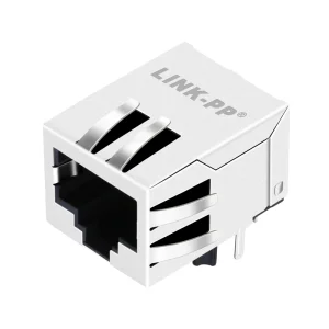
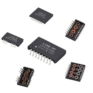
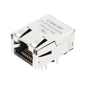
High-performance magnetic connectors, RJ45 jacks, and optical transceivers engineered to support robust physical layers in enterprise networking architectures.
How telecommunication leaders, system integrators, and hyper-scale data centers establish design, material, and electrical requirements for structured cabling ecosystems.
In modern telecommunication networks and enterprise IT facilities, the physical patch panel acts as the critical junction point that determines signal path reliability. Global procurement managers face complex design considerations, moving far beyond basic mechanical termination. Cable infrastructures must reliably support high-frequency transmission bandwidths up to 500 MHz (Cat 6A) or even 2000 MHz (Cat 8).
For custom OEM requirements, major system integrators mandate stringent performance benchmarks. Factors such as Near-End Crosstalk (NEXT), Return Loss, and Insertion Loss must be carefully controlled on the internal PCBs of patch panels to prevent network bottlenecks. When procuring panels for Power over Ethernet applications, contact engineering becomes critical. Standard contact materials can suffer from electrical arcing during connection/disconnection cycles under load, emphasizing the need for 50-micro-inch gold-plated interfaces and specialized design approaches.
IEEE 802.3bt (PoE++) systems transport up to 90W-100W of power. Custom RJ45 patch panels must incorporate superior heat dissipation designs and high-grade plastic polymers to resist thermal degradation inside wire bundles and port matrices.
Leveraging state-of-the-art diagnostic platforms, deep material engineering, and global logistics structures to supply network connectivity components.
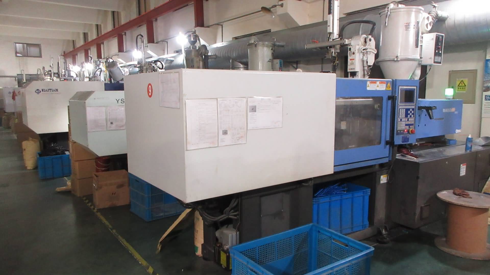
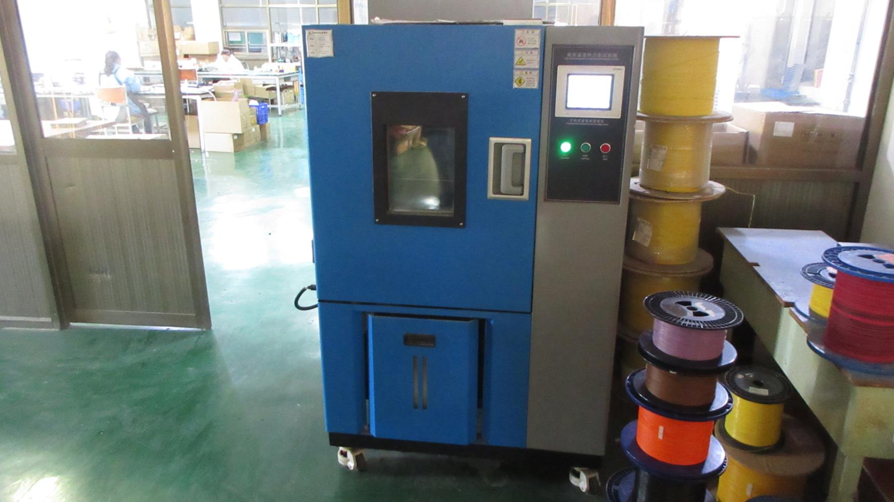
Founded in 2017, Equip-Link Intelligent Equipment (Shenzhen) Co., Ltd. is a specialized manufacturer and exporter of high-performance physical layer connectivity infrastructure and high-speed active components. While maintaining research and quality management workflows across our optimized 380 square meter facility, our robust ecosystem leverages a supply chain network of over 1,280 qualified partners. This extensive footprint ensures highly scalable production capacities, allowing us to supply system integrators, telecommunication networks, and data center infrastructures across 50 countries in North America, Europe, Southeast Asia, the Middle East, and South America.
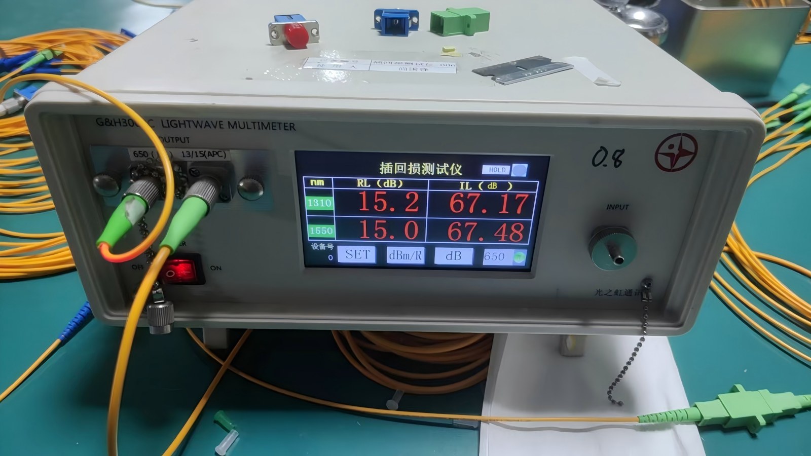
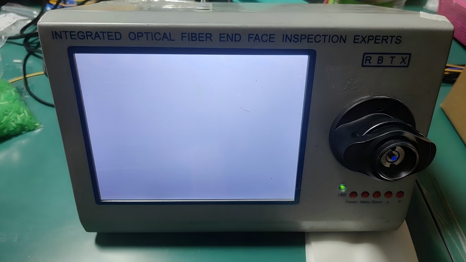
Our commitment to engineering quality is backed by a quality assurance team consisting of 36 experienced inspectors. From raw materials testing to final electrical analysis, every production run is tracked. To support evolving market requirements, our R&D group successfully developed and launched 126 new products in the past year, expanding our catalog of copper and fiber systems to keep pace with changing standards in cloud computing and AI infrastructure architectures.

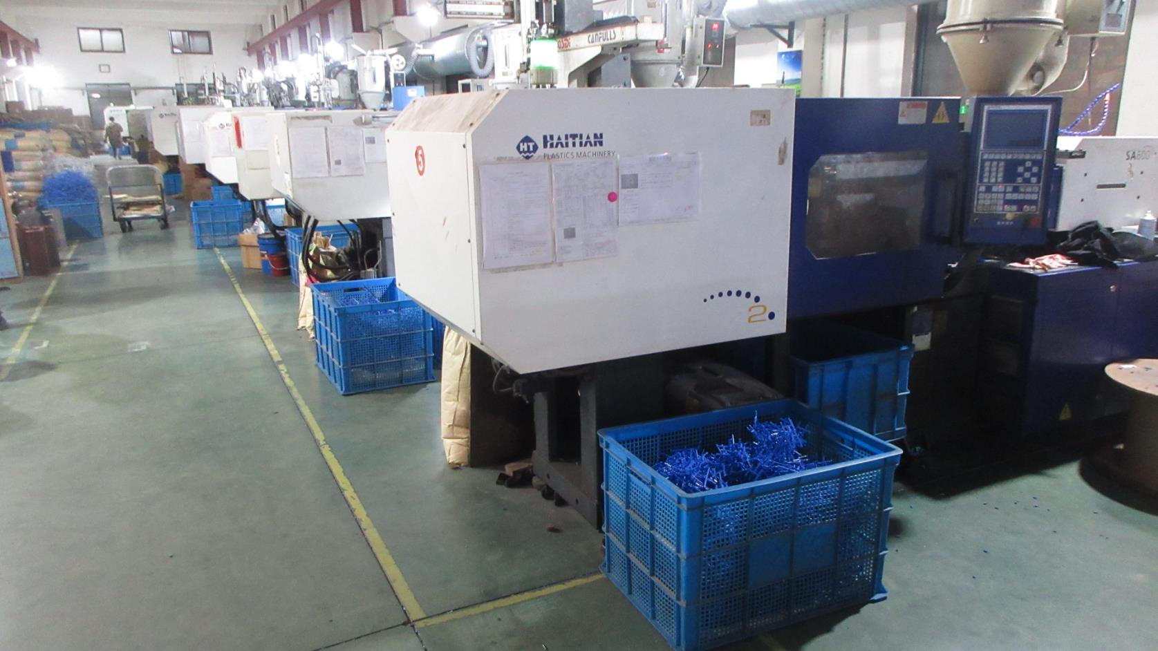
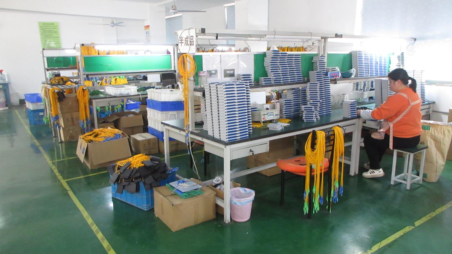
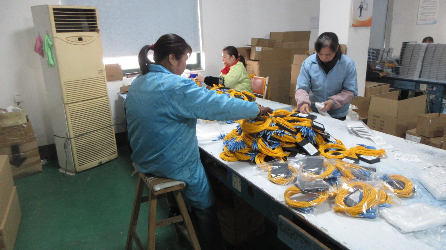
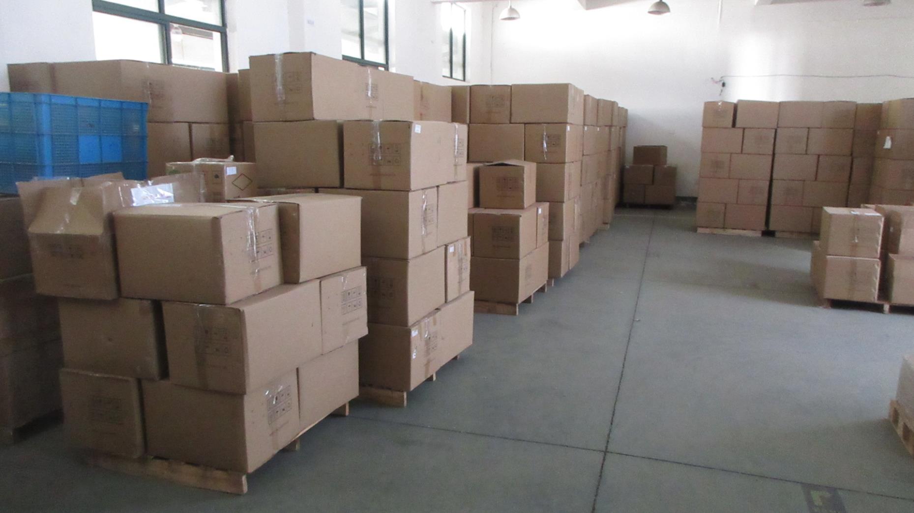
Bridging the gap between physical layer terminations and high-speed data transmission systems across key industrial verticals.
Supporting physical configurations where modular patch panels manage connections linking high-speed switches to servers. Designed to align with high-capacity optical transceiver uplinks for consistent network speed and bandwidth.
Providing carrier-grade distributions using shielded high-density panels to secure and route copper and fiber terminations, ensuring cross-connect efficiency inside central offices.
Deploying modular configurations supporting mixed media (Cat6A RJ45, fiber patch points, and multimedia keystone modules) to run gigabit workstations and centralized management setups.
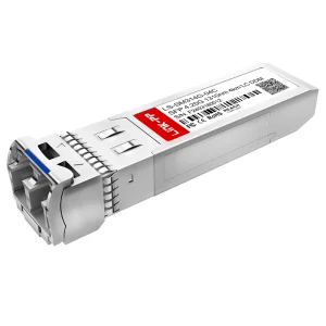
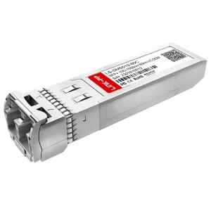
Modern network architectures require a balanced integration of high-bandwidth optical fibers and cost-effective copper connections. The interface between backhaul systems and distribution layers uses high-density RJ45 patching points alongside fiber components. For example, optical signals delivered through 10G SFP+ modules are converted by core switches and routed to terminal devices over structured copper lines via Cat6A patch panels. Our design engineering coordinates this overlap, helping ensure that shielding continuity, impedance matching, and ground connections are maintained across the entire network circuit.
A deep look at high-frequency signal design, modular mechanical layouts, and upcoming developments in structured cabling.
Our engineered patch panels utilize multi-layer PCB boards instead of point-to-point wiring to connect rear IDC terminals to front RJ45 ports. This structure allows precise track geometry layout, minimizing differential pair imbalances and controlling return loss. Compensating capacitive and inductive features are integrated directly into the trace layouts, canceling out phase errors and mitigating Crosstalk (NEXT/FEXT) to maintain headroom margins above industry standards.
Fixed all-in-one panels are increasingly being replaced by unloaded modular designs. System integrators can specify custom combinations of RJ45 connectors, fiber optic couplers, and coaxial interfaces on a single panel. This approach simplifies maintenance, allowing engineers to replace individual ports instead of replacing the entire unit.
Future infrastructure projects require real-time physical layer tracking. We are developing Automated Infrastructure Management (AIM) patch panels that feature built-in sensor contacts on every port. These panels track connection changes automatically, alerting administrators to physical link alterations through software interfaces to reduce downtime.
Our environmental design commitment focuses on raw materials selections. Standard plastics are replaced with Low Smoke Zero Halogen (LSZH) compounds and RoHS-compliant materials. Lead-free wave soldering processes are used for PCB production, ensuring that all components comply with international disposal regulations.
| Parameter | Category 6 Standards | Category 6A Standards | Equip-Link Engineered Performance |
|---|---|---|---|
| Maximum Bandwidth | 250 MHz | 500 MHz | Up to 650 MHz (Enhanced Headroom) |
| Alien Crosstalk (ANEXT) | Not Specified | Min. 50 dB @ 500 MHz | > 54 dB @ 500 MHz (Shielded Variants) |
| IDC Wire Termination Range | 22-24 AWG | 22-24 AWG | 22-26 AWG Solid/Stranded Wires Supported |
| Minimum Gold Plating Thickness | Selective Gold | 50 Micro-inches (Required) | 50 Micro-inches over Nickel barrier (Standard) |
| Insertion Durability | > 750 Cycles | > 750 Cycles | Verified > 1000 Mating Cycles |
Ensuring compatibility with international standards and providing local logistics and documentation support.
Our products are manufactured to meet standards including UL 1863, ANSI/TIA-568-C.2, ISO/IEC 11801, CE, FCC, RoHS, and REACH. This ensures cross-border entry compliance and simplifies site inspections by local safety officials.
We offer custom services including silk-screened logos, color-coded port configurations, private labeling, custom product designs, and tailored packaging layouts to align with your brand standards.
Every shipment includes testing reports from Fluke DTX/DSX analyzers, verifying compliance with return loss and near-end crosstalk requirements. Materials certificates are provided to verify traceability.
Addressing technical, logistics, and quality assurance questions from enterprise procurement buyers.
Under-plated contacts are vulnerable to oxidation, mechanical wear, and electrical corrosion, which leads to increased contact resistance and packet loss. 50 micro-inches of gold plating provides a durable barrier that protects signal integrity. This is especially important for high-power PoE applications (such as PoE++ Type 4), where un-plated interfaces can spark and corrode during connection/disconnection under load.
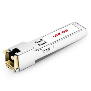
Our active modules and SFP transceivers undergo compatibility coding. We use a testing library that simulates the operational environments of over 50 leading network hardware brands. Optical testing instruments verify transmitter power, receiver sensitivity, and bit error rate performance.
Standard changes, such as custom branding, silkscreens, or labeling, are completed within 2 to 3 weeks. If you require custom metal casings or completely new PCB layouts, our design cycle requires 4 to 6 weeks for prototyping and validation, followed by 3 weeks for bulk production.
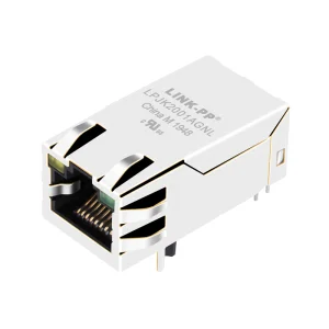
Yes, our punch-down modules and PCB trace terminals include color-coded labeling patterns for both T568A and T568B configurations. Dual-type IDC terminals allow termination using 110 or Krone impact tools, depending on installation preferences.
Fiber optic transceivers, modular jacks, and high-density copper interconnects engineered for high-performance networks.